Packaging is one of the most important processes in the LED industry. LED semiconductors are developed on what is called a wafer. Wafers are typically about five inches in diameter. The wafer is diced into thousands of microscopic pieces, each containing one copy of the circuit. Each of these microscopic pieces are called a die. These dice are picked off the wafer and placed into a reflective cavity and then a microscopic wire, called a bonding wire, is attached to the top of the semiconductor die and also to the positive lead, called the anode. After the attachment of the bonding wire an epoxy lens encapsulates the semiconductor.
There are primarily two types of LEDs, one called dual in-line package (DIP) and the other surface mount device (SMD). The DIP package is typically a single color and the SMD is typically three colors (RGB).
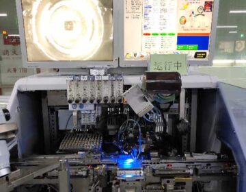
Once the LED has been packaged it is then ready to be put onto a tape or ribbon spool and is ready for placement on the circuit board.
GPS is constantly innovating new packaging designs and epoxy resins to increase the durability and color consistency. We work with new bonding wire formulas to enhance the connections and further drive down costs and improve quality.